
How to 3D Print Functional Prototypes for Consumer Electronics
Developing high-quality 3D printed prototypes for consumer electronics is the most effective way to validate ergonomics, internal component fit, and aesthetic appeal before moving to mass production. This iterative process allows designers to catch mechanical failures and assembly issues early, significantly reducing the financial risk associated with permanent tooling. By leveraging advanced additive manufacturing, brands can transition from a rough sketch to a functional, handheld device in a matter of days.
Why are 3D Printed Prototypes Essential for Consumer Electronics?
3D printed prototypes for consumer electronics are essential because they allow for rapid "form and fit" testing, ensuring that internal PCBs, batteries, and sensors fit perfectly within the enclosure. They provide a physical touchpoint for user testing, helping designers refine ergonomics and tactile feedback—like button clicks and port access—long before investing in expensive steel molds.
In my experience working with hardware startups, the biggest "aha!" moment always happens when a designer holds the physical part. I once worked on a wearable fitness tracker where the CAD model looked perfect. However, once we produced the 3d printing prototype, we realized the charging port was inaccessible when the strap was attached. Fixing that in CAD took ten minutes; fixing it in a hardened steel mold would have cost $15,000 and three weeks of delay.
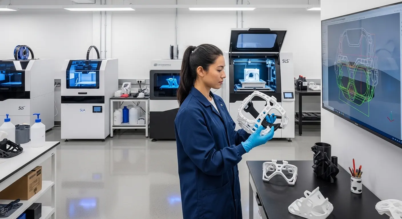
Which 3D Printing Technologies Best Suit Electronics Prototypes?
The best technologies for consumer electronics prototypes are SLA (Stereolithography) for high-detail enclosures, SLS (Selective Laser Sintering) for durable mechanical parts, and PolyJet for multi-material components like "overmolded" grips. Choosing the right method depends on whether you are testing the "look and feel" or the structural integrity of the device during drop tests.
| Technology | Best Use Case | Key Advantage |
| SLA (Stereolithography) | Aesthetic models, clear lenses, light pipes | Exceptional surface finish and detail |
| SLS (Selective Laser Sintering) | Snap-fits, hinges, structural chassis | No support structures needed; very durable |
| PolyJet / Multi-Jet | Soft-touch buttons, overmolded grips | Can print rigid and flexible materials together |
| FDM (Industrial) | Large enclosures, internal jigs and fixtures | Cost-effective for large-scale spatial mockups |
When should you choose SLA for electronics?
SLA is the gold standard for "Works-Like, Looks-Like" prototypes. If you need to simulate the smooth, glossy finish of an injection-molded smartphone case, SLA resins can be sanded and painted to be indistinguishable from the final product. It is also the only choice for light pipes and transparent screens where optical clarity is mandatory.
Why is SLS preferred for functional testing?
SLS uses nylon powder, which produces parts with high "fatigue resistance." This is critical for testing battery doors with snap-fit tabs or integrated hinges. When you compare molding vs. 3d printing, SLS parts come the closest to the mechanical properties of production-grade plastics, allowing for realistic assembly and usage testing.
How do you Select Materials for Electronics Prototypes?
Selecting materials for electronics prototypes requires matching the 3D resin or powder to the production plastic’s properties, such as ABS, Polycarbonate (PC), or TPU. For functional testing, engineers use high-temp resins for heat-generating components and "tough" resins to simulate the impact resistance needed for handheld devices that might be dropped during daily use.
Simulating Production Plastics
Most consumer electronics are made from ABS or PC/ABS blends. To get an accurate test, I always recommend using "Tough" or "Durable" resins in SLA. These materials are engineered to deform slightly before breaking, mimicking the way a real remote control or headphone frame behaves under stress.
Managing Thermal and Electrical Requirements
If your device has a high-performance processor, you must test for heat dissipation. Standard 3D prints can warp if they get too hot. In these cases, using High-Temp resins (which can withstand over 200°C) is necessary. Furthermore, if you are testing RF (Radio Frequency) transparency for Wi-Fi or Bluetooth, ensure your material choice doesn't interfere with signal strength—a common issue with certain carbon-filled filaments.
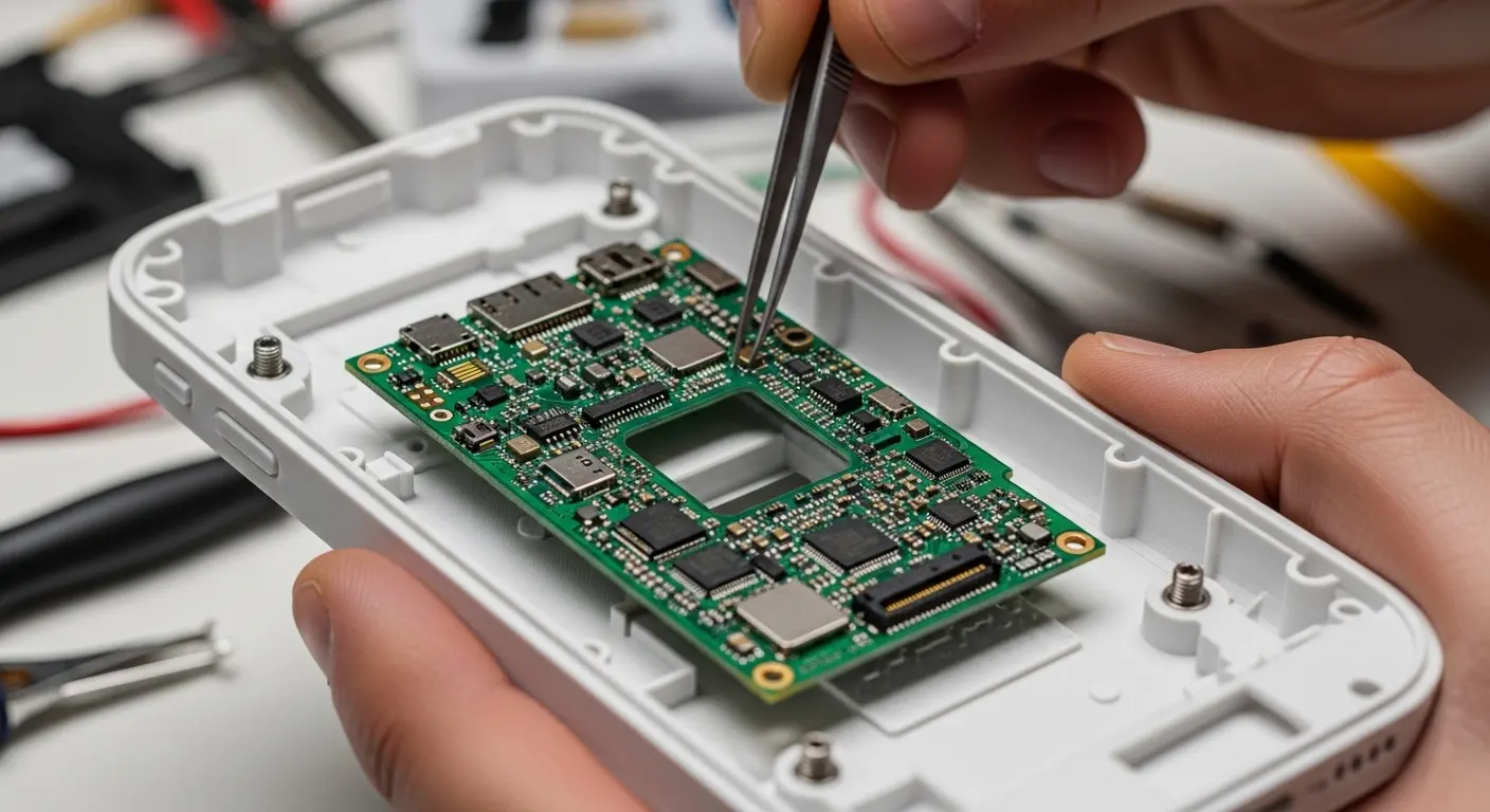
How to Test 3D Printed Electronics Enclosures?
Testing 3D printed electronics enclosures involves assembly verification, "Drop and Impact" simulations, and thermal management checks. Engineers physically install the PCB (Printed Circuit Board) into the 3D printed shell to check for screw boss alignment and clearance for heat sinks, ensuring the final assembly is both robust and manufacturable.
Tip: Always design your 3D printed screw bosses slightly undersized. This allows you to "tap" the threads or use heat-set inserts, which provide a much stronger connection for functional testing than simply screwing into raw plastic.
Verifying Snap-Fits and Clearances
One of the most common failures in consumer electronics is a "soft" snap-fit that doesn't stay closed. With low-volume injection molding, you usually get one shot at the design. 3D printing allows you to test the "clamping force" of your snaps. If the snap is too stiff, you can thin the geometry by 0.2mm and reprint the part in a few hours.
Environmental and Ingress Protection (IP) Testing
If your device is meant to be water-resistant (IP67), 3D printing is a great way to test gasket compression. While the 3D printed material itself might be slightly porous, coating it with a clear sealant allows you to perform vacuum or dunk tests to see if your seal design holds up under pressure.
How does 3D Printing Accelerate the Design to Production Pipeline?
3D printing accelerates the pipeline by allowing for "Parallel Engineering," where the enclosure design and the PCB layout are refined simultaneously. This reduces the need for "back-and-forth" redesigns, as physical prototypes can be shared with Top 10 Rapid Prototyping Manufacturers to identify potential manufacturing bottlenecks months before the production line starts.
Reducing "Time to Market"
In the electronics world, being first to market is everything. By utilizing Top 20 Rapid Prototyping Manufacturers, a company can have a fully functional "Beta" unit ready for trade shows or investor pitches while the final mass-production molds are still being cut in the factory.
What are the Design Constraints for 3D Printed Electronics?
The design constraints for 3D printed electronics include wall thickness limits, the need for support structure removal, and the inherent "layer lines" that can affect the fit of precision components. Designers must account for the "shrinkage" of certain resins and the orientation of the print to ensure that critical dimensions, like screen bezels, remain perfectly square.
Managing Wall Thickness
For most 3d printing technologies, a minimum wall thickness of 1.5mm is recommended for electronics. Anything thinner risks warping during the "post-curing" process. If you need a paper-thin aesthetic, you may need to transition to a more rigid material like a glass-filled nylon.
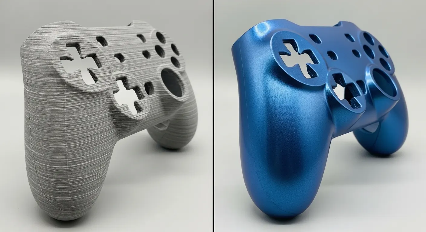
Post-Processing for High-End Aesthetics
A raw 3D print rarely looks like a finished consumer product. To achieve that "Apple-like" finish, parts must undergo:
- Sanding: Starting from 400 grit up to 2000 grit for a mirror finish.
- Priming and Painting: To hide layer lines and add UV protection.
- Vapor Smoothing: A process using solvent vapors to melt the surface of the plastic for a perfectly glossy, molded look.
Future Trends: 3D Printed Circuitry and Smart Enclosures
The "holy grail" of this industry is 3D printing the electronics inside the plastic. New technologies are emerging that allow for the "jetting" of conductive silver inks alongside structural polymers. This could lead to a future where a phone or wearable has no separate PCB; the circuitry is simply part of the 3D printed frame itself.
Furthermore, we are seeing more use of "Embedded Components." This is where a print is paused mid-way, a battery or motor is inserted, and the printer continues to build over it. This creates a completely sealed, tamper-proof device that is impossible to manufacture any other way.
Designing for Global Compliance and Safety
Even at the prototype stage, safety is paramount. Consumer electronics must eventually pass certifications like CE, UL, or FCC. Using UL-94 V-0 rated (flame retardant) 3D printing materials ensures that your functional prototype won't become a fire hazard during high-voltage testing or battery stress tests.
| Safety Factor | 3D Printing Solution | Benefit |
| Flammability | FR-ABS or Flame Retardant Resins | Meets UL-94 standards for electronics |
| ESD Safety | Electrostatic Dissipative (ESD) materials | Prevents static shocks from killing sensitive PCBs |
| Chemical Resistance | Polypropylene or Nylon | Survives exposure to skin oils and cleaning agents |
Final Thought
Developing 3D printed prototypes for consumer electronics is a strategic bridge between a visionary idea and a market-ready product. By selecting the right technology—whether it’s the aesthetic precision of SLA or the mechanical ruggedness of SLS—engineers can iron out every design flaw before a single dollar is spent on mass-production tooling. In an industry where consumer expectations are higher than ever, the ability to physically iterate, test, and refine a device in real-time is the ultimate competitive advantage. Additive manufacturing isn't just a tool for making models; it's the engine that drives modern hardware innovation.